COMPANY
INSIGHT
Sponsored by
Imaging Technology:
Expertise built on technology for space applied to missions on earth
Introduction
Performance is crucial in space technology, every successful generation in design represents a new state-of-the-art. Advancements proven in space may return to earth in unexpected places. Well-known examples are: satellite TV, water purifiers, freeze-dried food, and artificial limbs.
Caeleste is a Belgian fabless SME specialized in custom designed CMOS image sensors. The focus of its projects is very wide, yet in each project specs are “beyond state-of-the-art”. The company partners with world recognized institutions as the European Organization for Astronomical Research and the European Space Agency.
In this note we show how Caeleste re-used space mission results in sensors for the medical domain.
Space technology for medical applications
Space, although “empty” or effectively a deep vacuum, is not a benign environment. It is permeated with high-energy electromagnetic and particle radiation. This radiation is not only harmful to humans, it also destroys electronic devices. Caeleste has mastered to design its electronics resilient to the effects of radiation, or “radhard”. The damaging effect is seen as “total dose” and “single event” effects. Through many years of innovation, its image sensors and ROICs designs are successful in space missions.
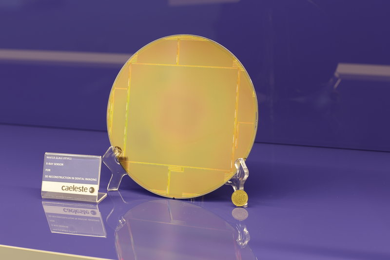
X-Rays are used in the most common forms of medical imaging. Our partnership with Trophy, part of Carestream Dental, is an example where Caeleste adds value in a domain where resilience against high energy radiation is required. We partnered in developing a new generation X-ray sensor for 3D reconstruction in dental imaging.
Unlike regular cameras, no lenses are used in X-ray imaging. Consequently, the size of an image sensor must match the size of the target area. This sensor measures 12 x 14 cm, or “wafer scale”. Caeleste’s IP made it possible to produce wafer scale devices with a high production yield.
This achievement for a medial application can be traced back to know-how acquired in space, and vice-versa. This systematic synergy of seemingly distance domains is unique for Caeleste. The technology that survives the space environment is applicable to many other forms of radiation; the high yield methods acquired in X-ray images apply on their turn to many other distant domains.
The expertise on low noise charge sensing circuits, originally acquired in deep cryogenic readout ICs (ROICs) for long wavelength infrared imaging, eventually led to the collaboration with the Californian med-tech startup Paradromics. Caeleste was part of a fundamental paradigm shift in the field of brain computer interfaces by developing a sensor for our customer that allows electrodes to be implanted into the brain at higher density than previously possible without causing thermal damage to the neural tissue. In addition, the sensor has an extremely challenging noise requirement to be able to read the neuron potentials. This is where craftmanship and passion for finding technological solutions were crucial for the success.
Solutions of this category cannot be purchased off-the-shelf and need to be developed by a team that has the expertise and the confidence to realize goals beyond what is available.
Providing solutions from a system-based perspective
Caeleste complements the sensor design with the driving system and the capability to do the full characterization. How the image sensor is used most effectively depends on the external system, and a sensor design is often a total system optimization. This impacts the presence, position and resolution of the ADC. It impacts on the amount and nature of image processing, on-chip, in-system, downstream. It involves design choices aiming to low noise operation, low power or high speed, high temperature or cryogenic temperature operation. The collection of know-how and IP enables us to design sensors for a variety of clinical applications such as ophthalmology, dental and mammographic imaging.
Additional information about Caeleste
For the development of a custom sensor Caeleste offers dedicated support after the design and testing process. To optimize the integration, Caeleste acts as a one-stop-shop for :
- Interacting with the Silicon foundry and related suppliers for post-processing
- Package design and manufacturing, glass lids, filters
- Optical Simulations
- Dedicated Coatings
- Driving electronics and boards
Caeleste’s partners are leaders in their respective fields such as: foundries, medical qualification specialists, testing houses, dicing and packaging experts.
If the needs of the customer change over time, we offer a collaborative approach and remain open to new possibilities. This describes our flexibility as a company but always with solid high-quality solutions in mind.